HBM Packaging Technology Divergence Explained – The Comprehensive Guide to Advanced Memory Packaging
High Bandwidth Memory has revolutionized the way we approach high-performance computing, artificial intelligence (AI), and gaming. The key to unlocking HBM’s potential lies in its packaging technology. While the basic principle of stacking multiple DRAM dies remains constant, the methods used to connect and integrate these layers vary widely.
This divergence in packaging technology has led to differences in performance, efficiency, and cost. In this article, we provide a detailed and easy-to-understand explanation of the various approaches and innovations that define the HBM Packaging Technology Divergence Explained topic. Our goal is to offer a definitive guide that not only informs but also serves as a strategic resource to help you gain a competitive edge.
Understanding HBM Technology
High Bandwidth Memory is a type of memory that stacks several DRAM dies vertically and connects them using advanced techniques. Unlike traditional memory types such as DDR or GDDR, HBM achieves significantly higher bandwidth while consuming less power. Over time, HBM has evolved through several generations—starting from HBM1, moving to HBM2 and HBM2E, and now onto HBM3 and even HBM3E.
Key Evolution of HBM
The evolution of HBM has brought several improvements:
- HBM1 set the foundation with basic stacking and TSV (Through-Silicon Via) interconnects.
- HBM2 increased capacity and speed, making it popular for high-performance GPUs.
- HBM2E introduced more layers and higher data rates.
- HBM3 and HBM3E now push the envelope with unprecedented bandwidth, lower power consumption, and innovative packaging techniques.
These advancements have positioned HBM as the memory of choice in data centers, gaming systems, and AI applications.
Basics of Semiconductor Packaging
Before diving into the specifics of HBM packaging divergence, it is crucial to understand what semiconductor packaging entails. Packaging is the process of enclosing the semiconductor die to protect it from physical damage and to provide the necessary electrical connections.
Traditional packaging methods, such as flip chip packaging, have evolved into advanced packaging techniques that include fan-out, 2.5D, and 3D architectures.
Comparison Table: Traditional vs. Advanced Packaging
| Aspect | Traditional Packaging | Advanced Packaging |
|---|---|---|
| Bump Pitch | 150-200 µm | 60-100 µm |
| Interconnects | Wire bonding, larger distances | TSVs, microbumps, direct bonding |
| Form Factor | Larger, less compact | Smaller footprint, higher integration |
| Performance Impact | Moderate speed, higher power use | High speed, improved power efficiency |
| Thermal Management | Limited, often external cooling | Integrated thermal solutions |
Advanced packaging has become essential as the performance gap between processing power and memory speed continues to widen.
Divergence in HBM Packaging Technologies
The phrase HBM Packaging Technology Divergence Explained captures the idea that companies are taking various routes to achieve the best possible integration of HBM with processors. Although the end goal is to provide high bandwidth and low latency, the techniques employed can differ significantly.
Why the Divergence?
The divergence arises due to multiple factors:
- Performance Requirements: Some methods, such as bumpless direct bonding, offer lower electrical resistance and improved signal integrity.
- Manufacturing Costs: Techniques vary in complexity and cost, leading some companies to opt for slightly less efficient but more cost-effective solutions.
- Thermal Management: Efficient heat dissipation is critical, and certain packaging methods allow for better thermal control.
- Yield and Scalability: Packaging solutions must also consider manufacturing yield and the ability to scale for mass production.
Companies like SK Hynix, Samsung, and Micron have all adopted different proprietary packaging strategies, each reflecting a balance between these factors.
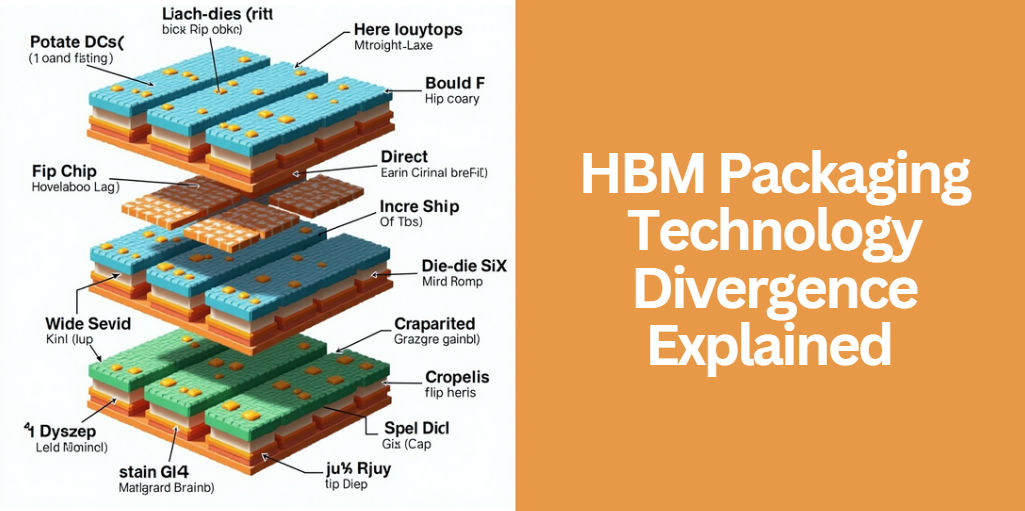
Deep Dive into HBM Packaging Methods
To better understand the differences, let’s explore the main packaging techniques used in HBM integration.
Interposer-Based Packaging
Interposer-based packaging involves placing the HBM stacks on a silicon interposer, which then connects to the GPU or CPU. This method offers excellent signal integrity and effective thermal management. However, the additional layer can increase manufacturing complexity and cost.
Key Features:
- Enhanced Signal Integrity: Due to shorter interconnect lengths.
- Improved Thermal Dissipation: Interposers help spread heat evenly.
- Cost Consideration: Higher manufacturing expenses due to extra processing steps.
Die-to-Die and Die-to-Wafer Bonding
Die-to-die (D2D) and die-to-wafer bonding utilize direct hybrid bonding techniques. The dies are bonded face-to-face (F2F) or face-to-back (F2B) with minimal intermediary layers. This method can significantly reduce parasitic capacitance and boost overall performance.
Benefits:
- Reduced Latency: Direct connections provide faster data transfer.
- Lower Power Consumption: More efficient electrical performance.
- Complexity: Requires high-precision alignment and bonding processes.
2.5D and 3D Packaging Architectures
These architectures take integration one step further. In 2.5D packaging, the memory dies and processing units are placed on a common interposer, whereas 3D packaging involves stacking active dies on top of one another.
Comparison:
- 2.5D Packaging: Balances performance and manufacturing ease.
- 3D Packaging: Maximizes density and minimizes footprint, but challenges with heat management and yield become more pronounced.
Technical Comparison and Trade-Offs
Understanding the technical metrics and trade-offs of each packaging method is essential for selecting the optimal solution.
Performance Metrics:
- Bandwidth and Latency: Direct bonding techniques typically offer the highest performance with lower latency.
- Power Efficiency: Advanced methods can significantly reduce power consumption compared to traditional packaging.
Cost Analysis:
- Manufacturing Complexity: More advanced techniques require higher precision and often result in increased cost per unit.
- Yield Considerations: Techniques that simplify the bonding process might offer better yield at the cost of slightly lower performance.
Thermal Management:
- Cooling Solutions: Integrated thermal solutions are critical for densely packed 3D architectures.
- Material Choices: The choice of interposers and bonding agents can impact heat dissipation.
Market Landscape and Competitive Analysis
The semiconductor market is highly competitive, with major players adopting different packaging technologies to gain an edge. Understanding the competitive landscape is crucial.
Industry Players:
- SK Hynix: Known for its high-performance and efficient HBM packaging strategies.
- Samsung: Invests heavily in innovative packaging techniques to boost bandwidth and power efficiency.
- Micron: Focuses on scalable and cost-effective solutions while maintaining competitive performance.
Strategic Insights:
Companies diverge in their approaches based on internal expertise, manufacturing capabilities, and strategic goals. The choice between proprietary and standardized solutions often depends on market positioning and target applications.
Case Studies and Real-World Applications
Real-world applications highlight the importance of advanced HBM packaging:
- AI and Data Centers: HBM is crucial for accelerating data transfer and processing in high-performance computing environments.
- High-Performance GPUs: Gaming and professional graphics applications benefit from increased bandwidth and reduced latency.
- Innovative Product Implementations: Several case studies illustrate how different companies have successfully integrated advanced packaging to achieve superior performance.
Example Table: Real-World HBM Applications
| Application Area | Key Benefits | Example Product |
|---|---|---|
| AI Servers | High bandwidth, low latency | NVIDIA Hopper H100 GPU |
| Gaming GPUs | Enhanced graphics performance | AMD Radeon series with HBM2E |
| Data Center Accelerators | Improved energy efficiency | Custom solutions from Micron |
Future Trends and Innovations in HBM Packaging
The future of HBM packaging is evolving with emerging technologies and increasing demand:
- Next-Generation Technologies: Innovations such as HBM3E and HBM4 are already in development, promising even higher bandwidth and better power efficiency.
- Role of AI in Manufacturing: AI and machine learning are beginning to optimize bonding processes and thermal management.
- Market Predictions: Industry experts predict a significant expansion in the use of advanced packaging technologies as applications become more demanding.
Practical Guide: Evaluating HBM Packaging Solutions
For system designers and OEMs, choosing the right HBM packaging solution is critical. Here are some practical steps:
- Identify Requirements: Consider the specific needs of your application in terms of bandwidth, latency, and power consumption.
- Cost-Benefit Analysis: Weigh the performance benefits against the manufacturing cost and potential yield issues.
- Integration Strategies: Evaluate how the packaging solution integrates with your overall system architecture.
- Future-Proofing: Consider scalability and compatibility with emerging technologies to ensure long-term viability.
Frequently Asked Questions
What Role Do Interposer Materials Play in Enhancing HBM Performance?
The selection of interposer materials is critical for optimizing electrical performance and thermal dissipation. Advanced materials such as silicon interposers with improved thermal conductivity and lower dielectric losses can significantly boost the efficiency of HBM stacks while maintaining high signal integrity.
What Are the Emerging Research Trends in HBM Packaging?
Researchers are exploring new interconnect materials and bonding techniques to push the limits of data transfer speeds further. Emerging trends include the integration of optical interconnects and the development of hybrid approaches that combine both traditional and novel methods to reduce latency even more.
How Does HBM Packaging Impact the Total System Cost Beyond Memory Performance?
The choice of packaging directly affects not only the performance but also the overall cost of system integration. Manufacturers must consider additional expenses related to specialized equipment, process yields, and quality control. These factors can influence the final price of high-performance computing systems in markets like AI, gaming, and data centers.
What Specific Challenges Arise When Transitioning From HBM2E to HBM3E Packaging?
Transitioning to HBM3E involves overcoming issues such as maintaining high yields with increased die layers and ensuring reliable bonding as the stack becomes more complex. Manufacturers also face challenges in optimizing thermal performance and aligning production processes with tighter tolerances required by the new generation.
How Do Advanced Packaging Techniques Contribute to Environmental Sustainability?
New packaging methods can reduce power consumption and improve energy efficiency, contributing to a lower overall carbon footprint. Additionally, some approaches aim to minimize material waste and enhance recyclability, making them a more environmentally sustainable option compared to older technologies.
Conclusion
In summary, HBM Packaging Technology Divergence Explained is a multifaceted subject that touches on the intricacies of stacking, bonding, and integrating high-bandwidth memory. This guide has provided a detailed exploration—from understanding the evolution of HBM and its various packaging methods to analyzing the market dynamics and future trends.
By comparing different approaches and highlighting their respective advantages and trade-offs, this comprehensive guide aims to serve as the ultimate resource for anyone looking to understand or implement advanced HBM packaging solutions.
Whether you are a system designer, a tech enthusiast, or an industry analyst, keeping an eye on these trends is essential to stay ahead in the rapidly evolving world of semiconductor technology.
More Posts
Ultimate Guide to News LoveLolaBlog: Your Comprehensive Resource for Digital Excellence
ATIS-100013.2007: The Definitive Guide to Telecommunications Standards
Ultimate Comprehensive Guide to the Sparkspitter Candle
The Ultimate Guide to Understanding and Tuning Ford 8.8 Track Lock S550 Ramp Angles
5StarsStocks.com: The Ultimate Guide to Stock Market Insights & Analysis